Pokazywanie postów oznaczonych etykietą science. Pokaż wszystkie posty

wtorek, 18 sierpnia 2020

OpenSPAD


OpenSPAD (Single Photon Avalanche Diode - fotodioda lawinowa do pomiaru pojedynczych fotonów) to otwarty detektor światła, działający na zasadzie zliczania fotonów przez fotodiodę lawinową pracującą w tzw. układzie Geigera z układem aktywnego gaszenia lawiny.

Projekt stworzony został przez elektroników z GaudiLabs [1], jako prosty w wykonaniu detektor zdolny do detekcji pojedynczych fotonów. Zastosowania takich detektorów są ogromne, głównie stosuje się je w nauce - w spektrometrii, mikroskopii, fizyce kwantowej etc. Dzięki temu, że układ ten jest w stanie wykryć pojedynczy foton i dokładnie zlokalizować go w czasie, diody tego typu stosować można także w eksperymentach czasoworozdzielczych, takich jak na przykład TCSPC (Time Correlated Single Photon Counting - czasowo skorelowane zliczanie fotonów) do mierzenia czasów zaniku barwników itp. lub HBT (Hanbury-Brown-Twiss, od nazwisk twórców metody) do korelacji emisji fotonów np. w celu wykrywania źródeł pojedynczych fotonów. O tych metodach bliżej może kiedy indziej. Teraz - kluczowy element - sam detektor fotonów.

poniedziałek, 21 grudnia 2015

Installing meep under Windows

I have decided to start some FDTD calculations or at least to learn how to calculate this. In order to omit all the problems with developing my own algorithms I have decided to search for a (preferably python) library doing FDTD stuff and found meep. The only problem with that is that it needs Linux and so I decided to use Cygwin instead. I was using this tutorial with some minor differences.

wtorek, 11 czerwca 2013

Short pulse generator, part 4.

As I have tested the device mentioned earlier (here) now I can show some pictures

The test setup
Short pulse generator entangled in wires

The device itself. The soldered twisted cable pair is for measuring the pulses before they hit the IXDD604 driver.

poniedziałek, 20 maja 2013

Short pulse generator, part 3.

Last week I have finally put together the pulse generator described earlier. IXDD604 driver seems to work in a satisfactory manner producing ~ 30 ns pulses. Unfortunately I didn't had time to make any photos of the working setup, so for now I can show you only a single pulse measured using 150 ohm load (a regular power resistor for now).


Sweet, isn't it? There are several issues still to be resolved like oscillations after the pulse (so called ringing) and difficulties obtaining such pulses for different amplitudes and loads. The problem, most probably, is in the pulse shaper not in the power driver so I should be able to pursue this in order to get this device working better than it is now.

czwartek, 9 maja 2013

Short pulse generator, part 2.

At last I have some time to write about recent progress in the matter of the short pulse generator. I have almost finished making the first prototype of this device. I had decided to use an integrated output stage. After some research I found IXDD604, and IC from IXYS that is dedicated as an MOSFET gate driver. Maximum voltage is 35 V and current a A, so it exceeds my needs in terms of power. 35 V peak amplitude must satisfy our needs at this moment, as this solution is very neat and I do not want to go into more complicated solutions as this should allow us to generate <30 ns pulses without any fuss.

The PCB is a single sided, as most of the elements are SMD. Only the driver is in THT as I was unable to obtain an SMD IXDD604 here. Such a design allowed us to make this PCB with thermotransfer and soon the prototype should be ready and soldered. I will post it as soon as I solder the prototype and run some tests.


piątek, 29 marca 2013

Short pulse generator, part 1.

Some time ago I have started designing an short pulse generator for time-resolved spectroscopy of electroluminescence. At first the design requirements were high, but after a market query, in search for devices capable of meeting these requirements they were lowered down significantly.

The sample for which this device is planned is a thin sheet of material suspended on an alumina frame, that acts as electrodes. We have measured DC I/V curve for the sample to assess the working parameters:


Therefore what we need is voltage of at least 35 V with current of at least 250 mA. In order to have an reserve in the parameters I assume that we need at least 40 V and 400 mA. For sake of simplicity I assume that the load of the device is almost purely resistive. Assesing the time parameters was a harder thing to do, so I assumes that the lower the better (the pulse time). Where is the limitation? In the power stage.

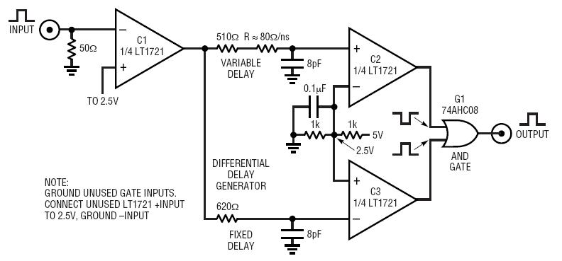
Using a simple generator, shown below, we are capable of generating a ~1 ns wide 5 V pulse with ease, using standard, from-the-shelf components. This could be even improved with faster ICs (comparators and AND gate.

From this Linear application note.

But this circuit generates only 5 V pulses (or close to that, this is the power supply voltage of the output AND gate). Also, the current is very limited - to 10 mA, offered by a TTL gate. In order to improve these parameters we have to add an output power stage, that will have output current and maximal voltage on the level of the planned device and could be controlled by an TTL pulse. To meet these requirements I have chosen several routes to achieve that:

  • A set of parallel bipolar transistor put in the common base topology. This should allow to achieve high rise and fall time of the pulse, but a current of a single fast transistor is low (tens of mA) so I need to put lots of them in parallel and I am not convinced that this is totally safe and will not affect the working of the device.
  • A (most probably single) FET/MOSFET device. An easy scheme for achieving high currents, even of hundreds of amps, but the pulse time will be significantly longer. With a dedicated driver and chip-to-pcb mount some people achieved 25 ns pulse width, although with a current of 100 A (as soon as I find the paper I'll post a link here). A stand-alone mosfet usually will have a rise time of several ns and fall time of 100 ns or more.
  • A dedicted IC. A RF power amplifier or a MOSFET driver. The first type of ICs seems to be a good idea as it offers tens of GHz in bandwidth, although when I have looked closer in this matter it seems that such IC will only work good in a typical circuit, for example an WiFi amplifier or so. On the other hand, some MOSFET drivers, are capable of almost meeting my requirements. EL7158 from Intersil is capable of producing 12 A pulses with rise and fall time of 12 ns (with 2000 pF load). This gives a chance to produce a 25 or shorter ns pulse, although the voltage is limited up to 18 V. Although this is not the only such driver on the market...
So currently I'm on the stage of parts requirements stage. As soon as I get something new I will post it here for sure.

piątek, 14 grudnia 2012

Electrode holder for a microscope

Today I finished making the blueprints of an electrode holder for an wide-field fluorescence microscope that we have at work. Nest week I'll take this to the workshop and I hope that they will quickly make the whole thing, so I can present it to you ;). And do some cool science of course.


I hope you like it. The electrode holder/manipulator consists of a base plate and top plate connected with springs and a micrometer head for controlling the height of the electrode that will be attached to the insulating teflon holder.

czwartek, 12 kwietnia 2012

Box for ammeter

Only a samll update today - a full metal enclosure for the ammeter I'm making at the moment. A nice render for the end of the day:


This will be milled from aluminum. You can see three holes for output, power and sample polarization voltage. There is also a hole for input connector on the other side. For input, output and sample polarization I plan to use BNC connectors, and for the power connector a dedicated three pin military-style connector. I hope to have this machined soon, so I can finish mounting the whole thing.

Also a dedicated sample holder will be milled from non conductive Teflon:


On this image you can see an additional set of clamps with golden needles attached. The needles are used to make an electrical contact with the sample.

piątek, 30 marca 2012

Vacuum chamber for optical spectroscopy part 3

Okay, so I've got all the parts for the vacuum chamber and assembled the whole thing.


I've started by assembling the window. It is a 3mm quartz plate, sealed with two rubber o-rings (that will be later replaced with fluoride rubber ones)


After that I've screwed down the windows part to the chamber body, sealing this joint with another o-ring. To the vacuum flange an vacuum valve was fitted (Leybold full metal manual valve).


So assembly is done, now for testing it we attached the chamber to pumping station consisting of a rough vacuum pump and turbomolecular drag pump. Pumping station is attached via an metal flexible hose. The pump was left for ~1h to evacuate the chamber.


After one hour of pumping we achieved pressure equal to 1,6 *10e-5 mbar. It is quite good result for that pump. On a normal cryostat pumped for an hour we achieve 5,4*10e-5 mbar, so the results are comparable (the cryostat is slightly bigger). The only one thing to test is the vacuum tight sealing. I'll take a look at the chamber after some time to see if it's still under vacuum.

Some new stuff just arrived

So, I've got some fresh stuff from the workshop. Still in as-received state, but this is a big step for now. Just see how blue-prints turn into reality:

PCB for the ammeter arrived! Not yet populated, as I'm still waiting for the ICs (should be here next week). I hope that everything will fit, as some drills are smaller than expected


Sample holder is also ready. It turned out very nice. Maybe not exactly as in the render, but the crucial parts are ok. Also it is blackened, to limit light scattering from it.


Also the vacuum chamber parts are done, but I still have to put it together - expect some pictures soon.

czwartek, 15 marca 2012

Sample holder

Some viewers say that I'm getting lazy. To prove them wrong, recently I've drawn a sample holder, that I need to fix my samples in my measurement setup. When everything will be finished I post some pictures of the whole thing, but now - only a drawing from Autodesk Inventor :).


This thing will be used to fix an microscope slide (3" x 1") in a 3 axis stage from Thorlabs. The stage is motorized using linear motorized actuators, also from Thorlabs. This will allow me to automatize a big part of my measurements. Stay tuned.

piątek, 9 marca 2012

Reduction ring

I love showing nicely rendered pictures of my projects :3 so here is a small, yet very important thing - an ring with threads, for thread reduction. Outer ring is SM1, and inner is M18. It will allow me to mount a prism in my spectroscope, and this means that I will hove to show it to you as soon as I finish constructing it.


Making these one made me learn how to configure a new thread in Autodesk Inventor, because the SM1 thread is not defined in the software. I anyone would be interested I could make a simple tutorial for that.

Spectrometer will consist of a prism, mounted via this adapter, an an iDus CCD camera. This device is a 1024x256 px camera, designed for use as an spectrometer. I will post some specs later on, when I will show the whole device.

poniedziałek, 5 marca 2012

Precise ammeter part 2 1/2

I've found a better op-amp for I/V conversion - OPA129. This one has similar parameters to the LMC6081, but allows for using +-15V power supply, and swings up to 13V output. This means that for 10Mohm R1 resistor I can swing up to 130nA, and measure as low as 200pA (due to the fact that offset voltage of OPA129 is 2mV).


To lower the offset voltage at the OPA129 output I've used an datasheet-suggested offset correction, that consists of R5, R6, R7, R8 and C9. It allows to trimm the offset using a potentiometer R8. If this will allow to nullify the offset, I guess it should allow me to measure the current and order of magnitude lower, down to ~50pA, or even less - depending on how effective the offset correction will be.
The PCB design is not varying much from the previous one. I've only adjusted several things to match the requirements of the company that is making the PCB. The order was sent to them so in ~2 weeks I should have the board in my hands. I also ordered some elements for the board, including the most important ones: R1 and R3. As R1 I choose 10M 1% Beyschlag resistor with low temperature coefficient - only 50ppm. R3 is 20k 0,1% 15ppm resistor.
As I calculated Vout = Iin*R1*(R4)/(R3), as R4 consists of a resistor and a potentiometer I assume it will be exact 200k. With the said resistors I will get Vout=Iin*10^10, this means 1 volt per 100pA. R1 error is 10^9*1% = 100k and R3 error is 20R. Without temperature effects (when the circuit will be maintained at 25*C) measurement error equals to Iin*1,1*10e6. This is six orders of magnitude lower than the measurement, which is Iin*10e10.
As I want to limit the bandwidth at around 10kHz I'll have to calculate the capacitance of C1 and C8. C1 calculated is 1,6pF and C8 is 79,6pF. Closest values are 1.5pF and 82pF, and such capacitors I bought to use in the final device.
I also ordered both op-amps, so I'll have to wait only for all the parts to come and then I can solder the circuit and do some tests, so stay tuned.

czwartek, 1 marca 2012

Precise ammeter part 2

There has been some work done with the design of the picoammeter (I guess it can be called so). There were some slight changes in the schematic and PCB design. I guess that the first stage is nearing to an end.
I've removed R2 from the non-inverting input of the IC1, as there is no need for using it in a symmetrical supply design, and added capacitor in the feedback loop of the IC2A, to filter out any high frequency noise that might be generated in the first stage.

Most of the tracks were thickened up to 0,032 inch where possible and last, but not least, I've added a guard ring around the input of the IC1, what is, I guess, crucial for measuring lows currents (at least ALL application notes and datasheets say so and I do believe in that).

Bottom layer of the PCBTop layer of the PCB
 The board will be made at a professional workshop, with metalization and gold plating.
Bottom view render of the PCBTop view render of the PCB

Finishing the schematic and PCB design I did some calculations. In order to finish the project stage I've calculated the elements I'm going to use. Most important part - R1 - will be precise 1GΩ ± 1% or 10MΩ. Unfortunately I have not found (yet?) any ± 0,1% resistors with such big resistance, but I guess this will not be a big issue and we can deal with 1% error. For this resistance I will get 1mV/pA. The offset voltage of the LMC6081 is in order of 1mV, so I guess that minimum measurable current will be in order of tens of pA (counting in the noise etc). Maximum current is limited by maximum voltage output of the op-amp, +5V powered is around 4,7V which gives 4,7nA for R1=1GΩ maximum current for the given supply voltage. If I exchange the resistor with 10MΩ the range will shift to 1nA - 470nA. Unfortunately there is no 100MΩ resistors at my main supplier. Will have to evaluate this more.
The second part, consisting of the OPA2227 should work with gain around 10. With 20kΩ input impedance this means R4 around 200kΩ, which is very reasonable value, if you ask me. The main problem with this part is also output swing. As I'm planning to use the same supply as for the IC1, the output will be similarly limited, as the OPA2227 does not have rail-to-rail output. I can always use higher power supply voltage, but this will complicate the design much.
The dynamic part of the calculations is to be made, as I don't know at which frequency I should limit the bandwidth. Looking at datasheet for the LMC6081 I'm guessing somewhere around 1kHz. This should give reasonable settling time of the measurement and slightly lower the noise.
I would like to thank Mr. Michał Penkowski, from Gdansk Technical University for lots of information and help about such measurements.
Still lots of work to be done!

środa, 29 lutego 2012

Vacuum chamber for optical spectroscopy part 2

I've got some input from my friends and, what's more important, bosses approval of this project. Here it is how the chamber project looks like now (nice render isn't it?)


Now I'm making technical drawings from this to have it turned and milled at the workshop. This will be made from aluminum (unfortunately, as this is vacuum equipment and should be made from stainless steel), with quartz window and fluor-rubber o-rings for sealing.

wtorek, 28 lutego 2012

Precise ammeter - the begginig.

I've started recently designing an ammeter that would be suitable for measurement of very very very low currents. Probably at the level of 1..100 nanoamperes. I need such device for measuring photo-current at work. Currently the project looks like that:


First IC is LMC6081. This is an precision CMOS Operational Amplifier, the main advantage of this op-amp is its very high input impedance (it needs only 10fA for biasing, geez, how do they measure it?!?) and low offset voltage. In this application it works as an I-to-V converter. Bandwidth of this op-amp is limited by C1.
Second op-amp is an low noise precision op-amp that will be used for amplifying the output voltage to measurable level (with 1Mohm measuring resistor R1 the output of the I/V converter is 100mV for 100nA). Second part of the OPA2227 is just an buffer to provide stable output.
PCB design is a real pain in the neck, at the current moment it look like so:


I don't have any idea how to optimize it more, especially to lower any leakage current that might change the measurement. I'm counting for some creative input of several people that I've asked to help me design this module. I hope to post some more info soon.

piątek, 24 lutego 2012

Vacuum chamber for optical spectroscopy

I started designing an vacuum chamber for our spectroscopy setup at work to measure fluorescence at low pressure. I would like to share with you some early plans of it. This is an image that I made using Autodesk Inventor to show how it may look finished.


The body will be made of aluminum, the windows (far on the left) probably quarz. The NW25 flange on top is for connecting a vacuum valve and pump.

I hope my boss will like it :).