Strony

piątek, 14 grudnia 2012

Electrode holder for a microscope

Today I finished making the blueprints of an electrode holder for an wide-field fluorescence microscope that we have at work. Nest week I'll take this to the workshop and I hope that they will quickly make the whole thing, so I can present it to you ;). And do some cool science of course.


I hope you like it. The electrode holder/manipulator consists of a base plate and top plate connected with springs and a micrometer head for controlling the height of the electrode that will be attached to the insulating teflon holder.

czwartek, 13 grudnia 2012

PC/104 DIO Card - final form

I have worked on the schematic of the digital I/O card based on the 82C55 for the SBC computer I have recently acquired and came with a final schematic - simplified as much as possible - and a PCB project. Here it is:


The schematic is simplified, yet it does comply with the PC/104 or ISA standard. There are three buffers - two for generic use - addresses and control signals (AEN, IOR, IOW, and RESET). Third buffer is utilized for data bus, and its control is a bit more tricky - the direction of the buffer is controlled by the buffered IOR signal and it is enabled by the ADDR signal that is generated in the addres decoder. For that part I have utilized a 8 bit comparator, so I can place the device in any address in the whole address space on 10 bits. Two LSB bits of the address are only buffered and feed to the 82C55 as it does all the magic. In that way I got rid of the strange address decoder of the old project and simplified generation of the Chip Select signal for the 82C55 - now it is selected by the ADDR signal from the address decoder.

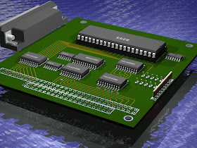
The board layout is now much simpler with enough space to fit and DC25 connector, like shown below.

I plan to send the project soon to have PCBs made and start soldering the whole thing. I have several ideas how to use this PC, but can not say anything for now. I'll keep you informed :).

wtorek, 11 grudnia 2012

New machines, new plans.

Recently - last weekend - I was gifted with two new machines for my collection. One of them is a VIA EDEN SBC in the 3,5" form factor and the second is a PICMG 1.0 single card PC with a Pentium MMX.

The first machine has various industry features, like 4 COM ports, PC/104 interface and a completely fanless cooling. I plan to build several cards for the PC/104 interface (starting with the DIO card seen below). This way I will have an powerfull, ethernet-enabled machine booting from an Compac Flash card for managing the I/O features of any system. Below is the photo of the current state of the motherboard with the heatsink. Not very impressive, isn't it?


The second PC that I was gifted with is a PICMG 1.0 processor card with a Pentium MMX CPU. Accidentaly I had such backplane and a dedicated rackmount housing for such a card. Below is a photo of the whole set - the card in the housing. Currently only the power is connected to the board, as I had time only to check if the card is alive. The next step is to complete the whole interior - FDD, CD and a 2,5" HDD. I will probably put an DIO card inside, or leve the only ISA/PCI slot empty and waiting for 'better times' ;-).


The inventory page of my blog is also updated a bit, there is a summary of all the machines I currently have. I revise it from time to time.

PC/104 format DIO card


As I have recently got a PC/104 capable PC (VIA EDEN) I have thought about putting together a small Digital Input/Output (DIO) board for this. In my spare parts I have found some of the famous Intels 82C55 chips and in the internet I have found a quite good looking schematic.

http://technologyinterface.nmsu.edu/4_1/4_1s.html


This kind of interface is a typical application of an ISA device - U1 - U3 are the buffers for the ISA interface, U7 is the address decoder and U9 - U10 generate the /CS signal for the 8255 for all the four addresses (8255 has four addresses - three for three 8 bit ports and one for control word). U10 seems to be a bit spare, so I decided to get rid of it and to add a switch for the address decode. Still it seems to be a bit complicated, but you really need all that glue logic to force it to work good. You can always interface it directly to the ISA, but this is highly unrecommended.


After having the complete schematic I started routing the board. So now the first problems emerged - It is really hard to fit all these ICs into PC/104 size format. Really, really hard. And not to mention to rout everything! so this is how it looks for now.


I have to redesign it completely I guess - rip-up every trace and start from scratch, as I have forgot to place the SUBD connector, and put everything into the same layer... this is not the best solution, especially when you are limited only to a double sided printed circuit board.

For sure I will post some more info when I finish redesigning the PCB.